|
Sample SPI drivers for a number of the Adesto Technologies flash devices.
|
|
Sample SPI drivers for a number of the Adesto Technologies flash devices.
|
The purpose of the Adesto Flash Driver Reference Package is to provide a source code reference for controlling and operating Adesto flash memory products. Using this package, users can understand how Adesto flash devices are controlled and operated, test their functionality, and get a starting point for developing their own drivers.
The current Adesto product families supported are:
The package, which is implemented in the C language, demonstrates most supported flash operations including memory reading, erasing and programming, control and status register reading and writing, and switching the flash device into various modes.
Communication with the flash devices uses SPI (Serial Peripheral Interface) and is implemented in bit-banging style. Bit-banging is the term for driving serial communication by host software directly manipulating SPI interface signals as general purpose I/Os rather than using a dedicated SPI hardware controller within the MCU. Since bit-banging can be implemented on any MCU almost the same way, the driver has very little dependency on the host MCU and as such is highly portable.
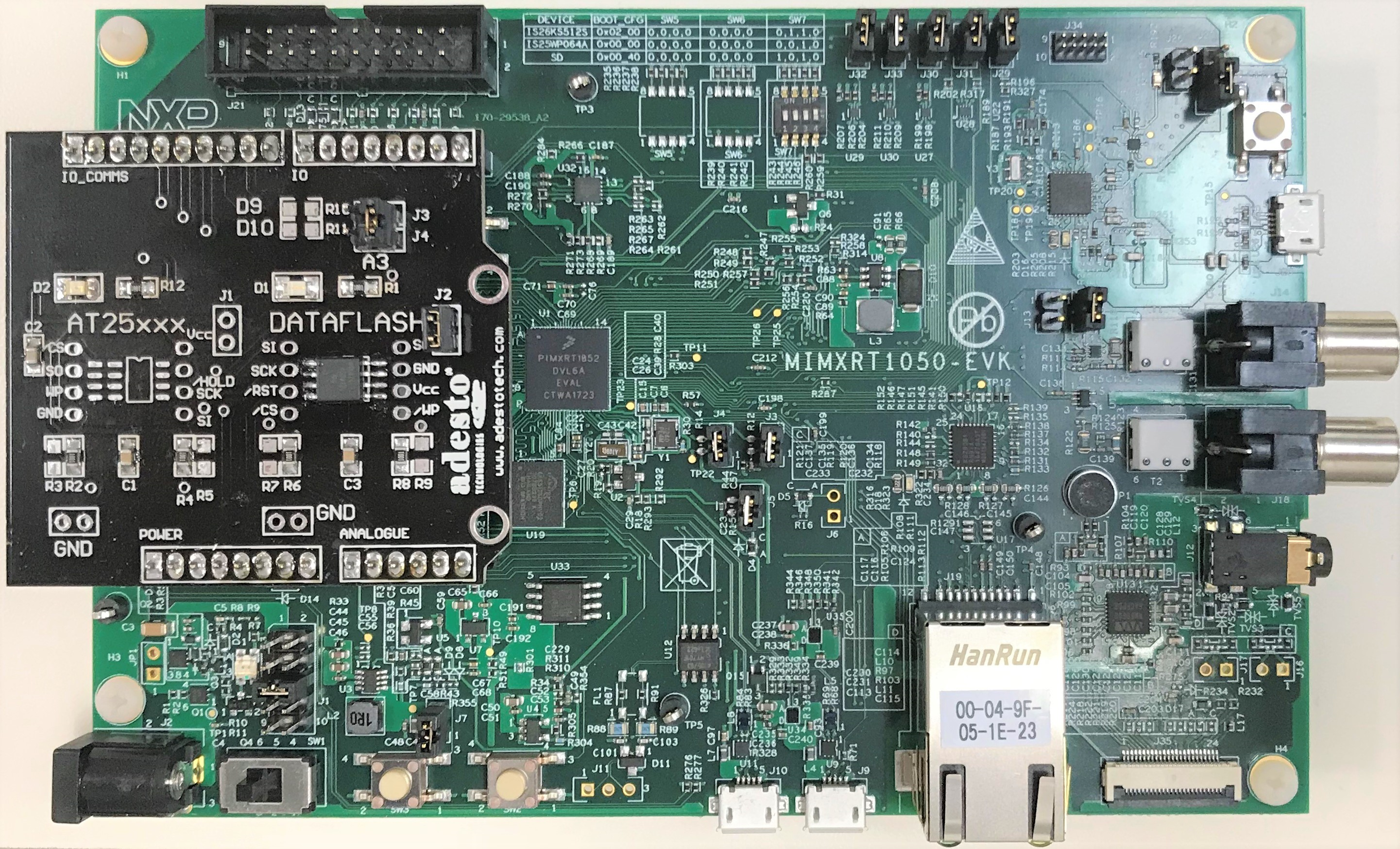
The source code was originally developed using the NXP MCUXpresso IDE and tested on a couple of NXP development boards:
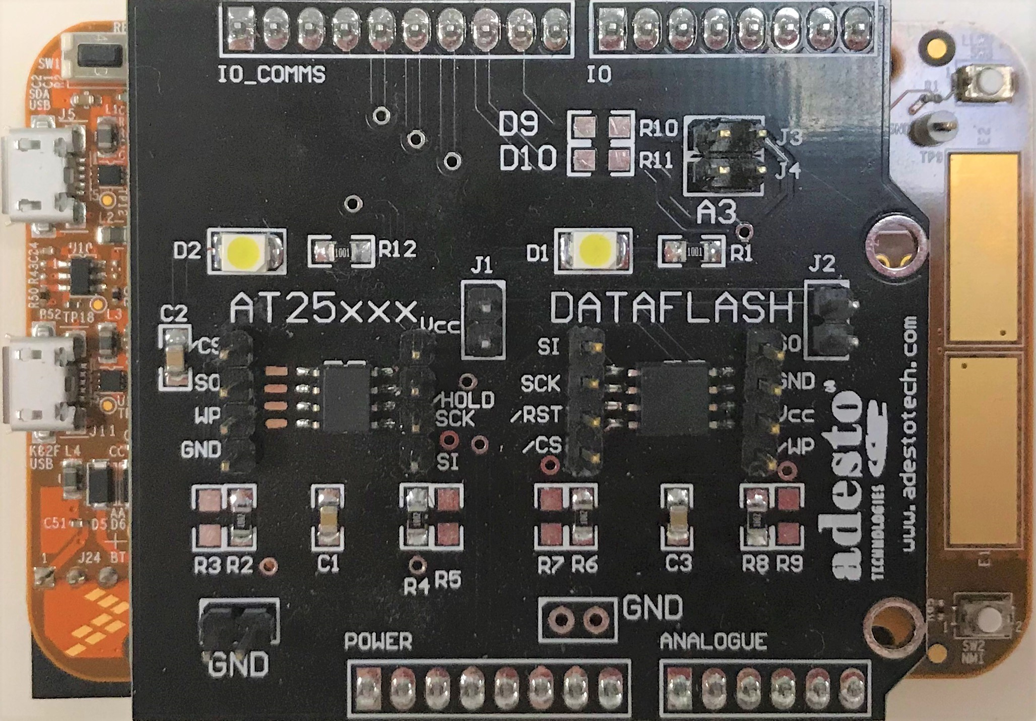
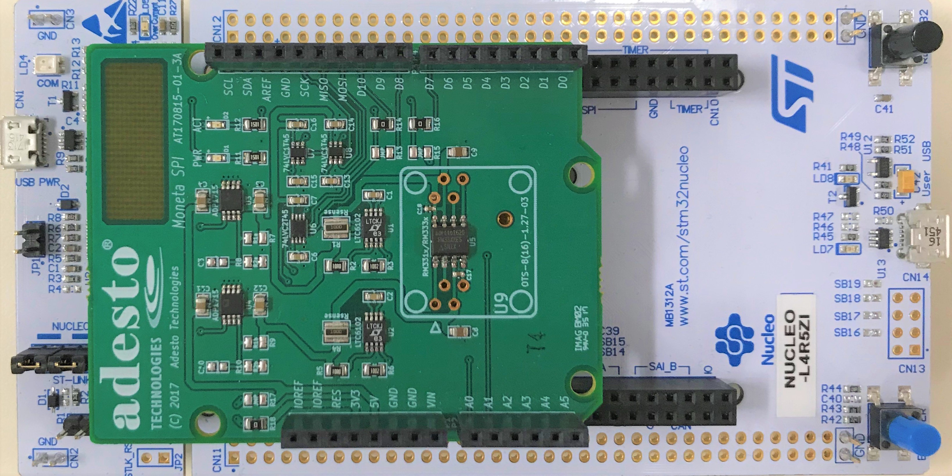
It was later ported to run on a ST Nucleo board (STM32 NUCLEO L4R5ZI). In all cases an Adesto-made "shield board" with an Adesto flash device was plugged into the host board. Using this configuration most Adesto flash products have been successfully tested. However the package is not limited to the hardware configuration used nor to the specific parts covered during testing.
The source code and documentation in html format can be downloaded from the github page. The downloaded archive file contains 2 folders; source and docs. As the names suggest, source contains the source code for the project, while docs contains the documentation. The source code is broken up into 3 sections as detailed in the Source Code Structure section.
The drivers can be used as reference material or ported to a MCU and used for testing. To run this project on a new board the user has to perform a relatively simple porting job by hooking the ports, pins, and initialization code to the specific MCU being used. This linkage occurs in the User Configuration layer (user_config.h, user_config.c). A comprehensive description on how to port the driver to a generic MCU can be found within this documentation at the User Configuration page.
After porting the User Configuration layer to work with a GPIO driver for the host MCU, the user must define the flash device used (see user_config.h). Defining the specific part used 'unlocks' the feature set offered by the drivers for that specific device. This is accomplished simply by typing the part identifier after PARTNO in user_config.h. The comprehensive test included with the code for each family of devices can then be run. The first test in the sequence reads the manufacturing ID and can give an early indication of successful communication. For more information about configuration see the User Configuration documentation.
Users can write their own tests by either modifying the source code, or adding in their own tests in test(). Specifically, the original package has a default test function that changes based on the part used. In a nutshell that test function (defaultTest()) sends a sequence of commands to the target and verifies the results, trying to cover as much functionality as possible. However, users may want to try their own test sequence by replacing the code in that test function with their own, or writing a new one in test(). See the Test Layer page for more information.
The source code and documentation can be downloaded here.
There are 4 main functional components to the Adesto Flash Driver Reference Package.
Together, these 4 components allow the user to port and test most of the commands available for the implemented devices. The SPI and User Configuration layers are tagged within the code by either a "SPI_" or "USER_CONFIG_" at the beginning of each function call. Adesto layer functions begin with the device name (ex: monetaReadMID()).
User Configuration Layer - This layer has all the user configuration and porting options. Using the user_config.h and user_config.c files, the project can quickly be set to
More information on this is provided at the User Configuration page.
Test Layer - This layer contains the default and user test functions, as well as the family specific test functions. Users can call defaultTest() to run the included example functions. defaultTest()'s definition changes according to the part selected and defined for PARTNO. test() is not defined, and is available for the user to test their own command sequences.
Adesto Layer - This layer includes implementation of commands and other functions for each family of devices. The test function then calls these functions in a certain sequence to test the functionality of the device. The device family appears as the first portion of the camelCase function name (ex. monetaReadMID()), and the functionality of that command is evident in the second half of the function name; Read Manufacturing ID in this case. The documentation for each function lists a brief explanation of the function, as well as the actual opcode that's sent to the device. Sending and receiving data is done through the SPI layer.
SPI Layer - This layer controls the GPIO pins in order to send and receive data in bit-banging style. Communication is done solely through the SPI protocol. In addition there is a JEDEC reset function built into the driver (SPI_JEDECReset()) for those devices which support that feature. The user facing functionality of the driver allows the user to send and receive bytes through transmit and receive buffers with the SPI_Exchange() function. Note, the driver must be modified in order to port to another board. A porting guide is included with this documentation (User Configuration).

Debugging any issues can be done at all levels from examining waveforms to using a debugger with breakpoints. Conveniently included within the SPI and Adesto layers are functions to assist with debugging. Byte comparisons can be easily done with compareByteArrays() (see helper_functions.h), and a fully integrated debug print can be turned on and off with debugOn()/debugOff(). The SPI layer also includes support for a 'trigger' which toggles a GPIO pin through a falling edge (SPI_Trigger()), to assist debugging with a logic analyzer or scope.