|
Sample SPI drivers for a number of the Adesto Technologies flash devices.
|
|
Sample SPI drivers for a number of the Adesto Technologies flash devices.
|
The SPI layer is used as a SPI driver to communicate with the flash device. This is accomplished through the use of bit-banging. As such, the SPI layer is built on top of a functional MCU specific GPIO driver. Once a GPIO driver has been connected to this layer (see the User Configuration guide for a how-to), function calls from the Adesto or SPI layers should work. Code for the SPI layer consists of a header and c file which contain functions for single, dual, and quad SPI communication. Adesto layer commands access the SPI layer to communicate with the flash device. The SPI layer calls functions from the user configurable user_config.h and user_config.c files. See the User Configuration documentation for more details.
Reading and writing to the the IOs occurs after the falling edge of the clock but before the rising edge in the current implementation of the SPI drivers. This behavior can be seen within the SPI_ReceiveByte() and SPI_SendByte() functions where data is sampled or written, then the clock toggled from low to high.
Users are intended to access the larger SPI transactions functions which handle the order of bytes transmitted, configuration of the IOs, and bit/byte shifting. These functions allow the user to shape the SPI transaction to include dummy bytes and communicate portions of the message using 1, 2, or 4 IOs. These transactions are accomplished through the following 3 functions calls:
Documentation for each of these functions details how the specifics of each argument and how the transaction is carried out. In summary, the user passes in 2 byte arrays; one for trasnmitting and one for receiving. The user also specifies the number of bytes being transmitted or received from 0-N (N being determined usually by the page size of the device being used, but ultimately variable and dependant on what the user needs). The number of dummy bytes is also passed in, the value independant of the transmitted number of bytes. The dual and quad exchange functions include another parameter which determines the number of bytes from the MCU transmitted SPI exchange to be sent in single SPI (transmission along MOSI alone). This number must be less than or equal to the total number of transmitted bytes. With this variable the user can send a quad or dual communication in a range of formats from 1-1-2 to 4-4-4 or even 0-4-4 (opcode-address-data, values representing the number of IOs used in the transaction of each component). For example, a user wishes to send a 1-byte opcode along MOSI, a 3-byte address along 4 IOs, 2 dummy bytes after the address, and receive a 5-byte data packet along 4 IOs. This transaction would be classified as 1-4-4, and the corresponding function call would look like this:
The arguments in order are explained as follows:
Since only 1 byte is sent in standard SPI mode, all communication after the opcode is done with 4 IOs, including the dummy bytes. The transaction looks like this when viewed with a logic analyzer:
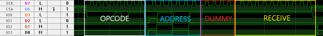
Note the number of clocks used for each portion of the transaction. For a 1-4-4 communication the opcode is clocked out 1 bit at a time, followed by a nibble on each clock for the address, dummy, and data bytes.